 点森科技 - 科技资讯_数码产品_互联网观察_智能硬件
湾芯展将于2026年10月14日至16日在深圳会展中心(福田)举行。展会同期,在第三代半导体国家技术创新中心指导下,由深圳市半导体与集成电路产业联盟、深圳平湖实验室共同主办的化合物半导体材料与工艺论坛将精彩启幕。
粤港澳大湾区汇聚新能源汽车、数据中心及科技应用产业,对化合物半导体和功率半导体技术形成旺盛需求。湾芯展将专设化合物及功率半导体展区与系列论坛,围绕化合物半导体及硅基功率半导体,集中探讨产业趋势、前沿技术、应用需求与工程化落地,邀请学术界和产业界嘉宾分享最新研究成果与实践经验。

产业生态合作伙伴


赞助合作

WESEMiBAY 2026
议程抢先一览

WESEMiBAY 2026
嘉宾阵容揭晓


演讲简介/亮点
新能源发电与储能、数据中心供电等应用急需高效率高功率密度碳化硅功率器件。汇报中高压碳化硅功率器件的性能能特点和发展趋势及其最新研究进展。
New-energy power generation and storage, and data center power supply demand SiC power devices with high efficiency and high power density. The performance characteristics, development trends and latest research progress will be presented on medium‑ and high‑voltage SiC power devices.


演讲简介/亮点
本报告围绕大尺寸单晶碳化硅,从电学、光学、声学、散热四个维度梳理材料特性、技术进展与产业应用。分析其在功率器件、AR光波导、声表面波(SAW)器件、先进封装散热等场景的差异化优势,剖析大尺寸衬底制备、加工面临的核心瓶颈,展望多领域广阔的产业化前景。
1. 多维物性视角:突破传统功率器件单一视角,覆盖电学、光学、声学、散热四大应用方向;
2. 多场景落地:兼顾成熟功率电子,拓展AR光波导、SAW声表面波器件、微流道散热等新兴方向;
3. 聚焦大尺寸痛点:剖析扩径、缺陷控制、高精度晶圆加工的现实挑战;
4. 产业前瞻:分析材料未来市场空间与技术迭代路径。
This presentation reviews the technical progress and applications of large size single crystal silicon carbide from four perspectives: electrical, optical, acoustic and thermal management properties. It analyzes its unique advantages in power devices, AR waveguides, SAW devices and advanced packaging heat dissipation. Key bottlenecks in largesize substrate fabrication and processing are discussed, together with broad industrialization prospects in multiple emerging fields.
1. Multi dimensional perspective: Cover electrical, optical, acoustic and thermalmanagement properties beyond conventional powerdevice focus.
2. Diversified applications: Combine mature power electronics with emerging fields including AR waveguides, SAW devices and micro channel heat dissipation.
3. Practical challenges: Address critical bottlenecks in large size expansion, defect control and highprecision wafer processing.
4. Industrial outlook: Forecast market potential and future technology evolution roadmap.


演讲简介/亮点
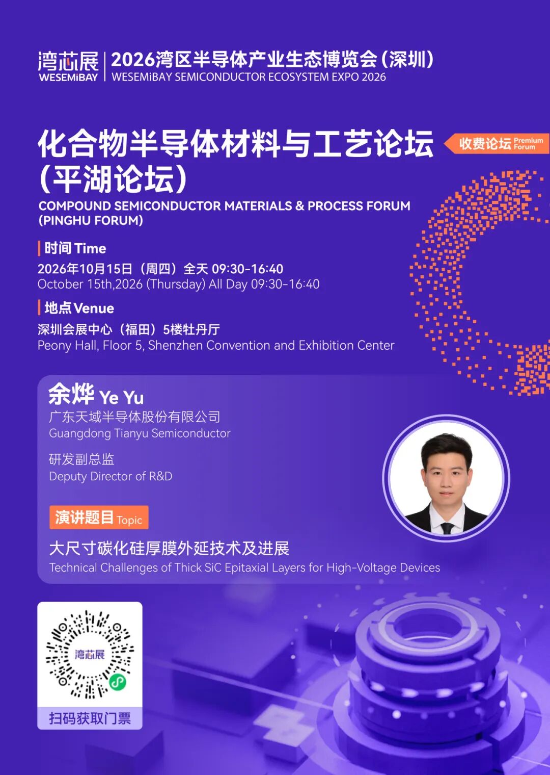
本次演讲介绍天域半导体在大尺寸碳化硅厚膜外延领域的技术攻关成果,重点阐述大尺寸厚膜生长均匀性、缺陷控制、应力翘曲抑制等核心难点,分享面向高压 / 特高压功率器件的厚膜外延工艺迭代进展,展示天域在 6/8 英寸大尺寸厚膜外延的技术能力与产业化落地情况,为高压 SiC 器件应用提供材料支撑。
This presentation will cover Tianyu Semiconductor’s progress in large-diameter thick SiC epitaxy, focusing on growth uniformity, defect control, and suppression of stress and wafer bow. It will review process improvements for thick epitaxial layers intended for high- and ultra-high-voltage power devices, and present Tianyu’s capabilities and industrial deployment of 6-inch and 8-inch thick SiC epitaxy to support high-voltage SiC applications.



演讲简介/亮点
人工智能市场正迎来空前繁荣,面对未来演进需求、数据安全以及兆瓦级数据中心的高能耗挑战,安全可靠的供电架构尤为关键。
本次演讲将围绕数据中心供电架构的演进,深度剖析从 35kV/10KV 高压输入到 AI 芯片供电链路的多种演进方向,核心功率器件的应用趋势和关键技术难题。
The artificial intelligence industry is experiencing unprecedented prosperity. Faced with future evolutionary requirements, data security concerns, and the high energy consumption challenges of megawatt-level data centers, a safe and reliable power supply architecture has become particularly critical.
This speech focuses on the evolution of data center power supply architectures, and conducts an in-depth analysis of multiple development trends throughout the entire power supply chain—from 35kV/10kV high-voltage input to AI chip power delivery, as well as the application trends and core technical challenges of key power devices.



演讲简介/亮点
随着 AI 算力爆发,AIDC 对服务器 PSU 的效率、功率密度、散热及可靠性提出严苛要求。本演讲围绕国产碳化硅功率器件在 AI 数据中心电源的工程化应用展开,结合图腾柱 PFC、LLC 等主流 PSU 拓扑,分析国产 SiC 器件关键参数对电源整机效率、EMC、可靠性的影响;对比 Si、SiC 器件在服务器电源不同工况下的表现,分享方正微电子国产 SiC 器件在大功率 AIDC PSU 的系统适配、调试要点与实测数据;探讨国产 SiC 器件面临的机遇与挑战,给出从器件选型、驱动设计到系统可靠性验证的完整落地思路,为 AIDC 电源国产化提供工程参考。
With the explosive growth of AI computing power, AIDC puts stringent requirements on efficiency, power density, thermal performance and reliability of server PSU. Focusing on the engineering application of domestic SiC power devices in AI datacenter power supplies, this speech analyzes how key parameters of domestic SiC devices affect overall powersupply efficiency, EMC and system reliability based on mainstream PSU topologies such as totempole PFC and LLC resonant converter. It compares the performance of Si and SiC devices under different operating conditions of server power supplies, and presents system adaptation tips, debugging guidelines and test data of FMIC domestic SiC devices deployed in highpower AIDC PSU. Opportunities and challenges for domestic SiC devices are discussed, delivering a complete implementation workflow covering device selection, gatedrive design and system reliability verification, which provides practical engineering references for the localization of AIDC power systems.


演讲简介/亮点
随着4H-SiC的应用扩展至智能电网、海上风电等超高压功率器件领域,开发高质量的4H-SiC超厚外延薄膜已成为4H-SiC同质外延的发展趋势。本工作首先提出降低热壁高度以改善超厚4H-SiC外延薄膜的掺杂均匀性,建立了超厚4H-SiC同质外延层的生长窗口,该窗口确保了稳定的台阶流生长。结合热场与流场优化、晶圆级掺杂均匀性改善以及缺陷控制,我们最终获得了厚度超过300 μm的超厚4H-SiC层。晶圆级掺杂均匀性低至8.29%,形貌缺陷密度降至0.75 cm⁻²。


演讲简介/亮点
宽禁带半导体氮化镓(GaN)具有禁带宽度大、击穿场强高、电子饱和速度高等特点,特别适合制备中低压、高频、高效功率电子器件,在消费类电子、机器人、数据中心等电源管理系统有着广泛且重要的应用前景。本报告将重点讨论硅基GaN增强型HEMT的可控制备及栅极可靠性加固技术。
GaN-based semiconductor has a wide band-gap and holds a great potential for power electronics applications. This talk will discuss about the key challenges and recent progress of GaN-based enhancement-mode high electron mobility transistor (HEMT) with a p-GaN gate, including the gate recess and p-GaN overgrowth, as well as the related reliability issues. In particular, a thin GaN layer is inserted within AlGaN barrier to facilitate the reproducible fabrication of recessed gate with a uniform depth and an ultra-low density of interface states. The thin GaN interlayer is also found to beneficial to mitigate undesired charge accumulation at the interface and significantly improve the p-GaN gate reliability.


演讲简介/亮点
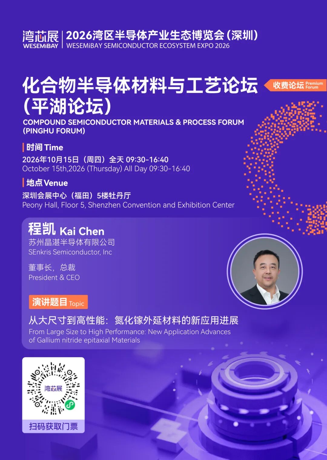
GaN被认为是下一代电力电子与新型显示技术的核心材料,尤其在新能源汽车领域,转换器、OBC、数字座舱等都得到了市场的广泛关注。
晶湛半导体提供的高质量硅基GaN HEMT外延片,可涵盖40—1200V功率应用;并在全球首次将GaN-on-Si晶圆尺寸成功扩展至300mm。同时,晶湛创新开发并实现的多沟道结构、垂直结构、GaN/SiC混合系统等多种新型外延结构,极大拓展了GaN在高压领域的应用潜力。
此外,晶湛半导体也为AR/VR等新型显示应用提供性能优异的、大尺寸硅上Micro-LED全彩(RGB)解决方案。晶湛半导体的300mm大尺寸硅基GaN外延片,为先进的功率、射频、光电芯片与逻辑芯片的混合异构集成铺平了道路。
GaN is considered to be the core material of the next generation power electronics and novel display, especially for the application like EV, converters, OBC, digital cockpits, etc.
High-quality GaN-on-Si HEMT epitaxial wafers offered by Enkris Semiconductor, Inc. can cover 40-1200V BV applications; Enkris is the first supplier which successfully extend GaN-on-Si wafer size to 300mm. At the same time, Enkris innovatively developed and realized a variety of new epitaxial structures such as multi-channel structure, vertical epi-structure, and GaN/SiC hybrid system, which greatly expanded the application potential of GaN in HV applications.
In addition, Enkris also provides high-performance, large-size GaN-on-Si Micro-LED full-color (RGB) solutions for novel display such as AR/VR. Enkris’ 300mm large-size GaN-on-Si epitaxial wafer paves the way for the hybrid heterogeneous integration of advanced power, RF, optoelectronic chips and logic chips.



演讲简介/亮点
随着 GaN 器件向大尺寸晶圆与规模化制造演进,业界对低成本、易整合的外延方案需求日益迫切。本次演讲将介绍 Evatec 基于溅射的 PVD GaN 技术路线,探讨其作为 MOCVD 互补方案在量产中的价值:无需金属有机前驱体,显著降低设备与运营成本、简化厂务配套;低温工艺降低热预算与晶圆应力,更易与 CMOS 兼容工艺结合;无氢环境支持高浓度掺杂,满足低阻接触层需求。


演讲简介/亮点
本演讲将系统梳理GaN材料的主要应用领域,分析不同应用对GaN外延提出的关键要求,并分享中微公司在这些领域的MOCVD解决方案。重点环节将介绍面向GaN基HEMT外延的新型MOCVD设备Preciomo Udx/Pdx,以及该设备的最新研究进展,帮助听众了解GaN外延设备的技术趋势与产业化进展。
This presentation will systematically review the main application areas of GaN materials, analyze the key requirements that different applications place on GaN epitaxy, and share AMEC’s MOCVD solutions in these fields. A key part of the presentation will introduce the new MOCVD system Preciomo Udx/Pdx for GaN based HEMT epitaxy, along with the latest research progress achieved with this system, helping the audience understand the technology trends and industrialization progress of GaN epitaxy equipment.



演讲简介/亮点
AI算力爆发推高数据中心功耗,传统供电架构面临效率与功率密度瓶颈。本演讲将分享英诺赛科在氮化镓器件上的最新进展,解析GaN如何凭借高效、高频、高功率密度优势,在AI数据中心实现系统级能效跃升,助力AIDC建设。


演讲简介/亮点
功率氮化镓(GaN)技术因其在高能效、高功率密度功率电子系统领域的独特优势,正成为推动800V算力中心供电技术革新的核心驱动力。本次报告将系统阐述15V-1200V功率GaN与集成技术在算力中心全链路供电等领域的应用前景,并深入分析其对GaN器件的关键技术需求。随后,报告将聚焦8英寸15V-1200V功率GaN最新研究进展,包括GaN外延、关键工艺、器件以及单片集成等技术领域。最后,展示深圳平湖实验室8英寸功率GaN研发中试平台建设及技术规划。
Power GaN technology is emerging as a core enabler of the 800V power-supply revolution for AI data centers, owing to its unique advantages in high-efficiency, high-power-density power electronics. This report will systematically present the application prospects of 15V–1200V power GaN and integration technologies across the full power-delivery chain of AI data centers, and will analyze in depth the key device-level requirements for GaN. It will then highlight the latest advances in 8-inch 15V–1200V power GaN, covering GaN epitaxy, key process modules, devices, and monolithic integration. Finally, the construction and technology roadmap of the 8-inch power GaN R&D pilot platform at Shenzhen Pinghu Laboratory will be introduced.



演讲简介/亮点
1.GaN HEMT器件动态测试面临的挑战;
The challenges in dynamic Testing of GaN HEMT
2.GaN HEMT器件动态测试技术分享;
The sharing on dynamic parameters testing of GaN HEMT
3.GaN HEMT器件动态测试示例;
The examples for dynamic parameters testing of GaN HEMT
4.GaN HEMT器件DHTOL试验能力介绍。
The Introduction to DHTOL testing for GaN HEMT
WESEMiBAY 2026
10月相聚深圳湾芯展
诚邀学术界、产业界与投资界的专业观众莅临现场,与嘉宾共同交流化合物及功率半导体领域的技术进展、应用机遇与产业实践。

扫码加入论坛交流群
*更多嘉宾及议程信息将陆续公布,最终安排以现场公布为准。欢迎扫码加入论坛交流群,及时获取议程更新与现场动态。


点击“阅读原文”,快速进入湾芯展观众报名通道!